Micro-Particulate and Gaseous Contamination Mitigation
In semiconductor microchip fabrication and OLED panel assembly, contamination is measured at the nanometer and sub-ppm level. A single micro-particle of airborne dust landing on a photoresist wafer layer can cause path breakages, reducing wafer yield.
Industry Challenges
- Particulate Control: Maintaining an environment free from microscopic airborne dust during substrate transport.
- Electrostatic Build-up: Dry nitrogen environments generate static charges, attracting dust and causing ESD damage to sensitive microchips.
- Interface Integration: Safely transferring samples between atmospheric glove boxes and ultra-high vacuum ALD or deposition chambers.
The BET Solution
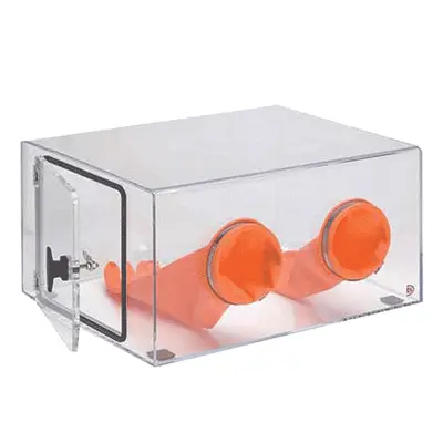
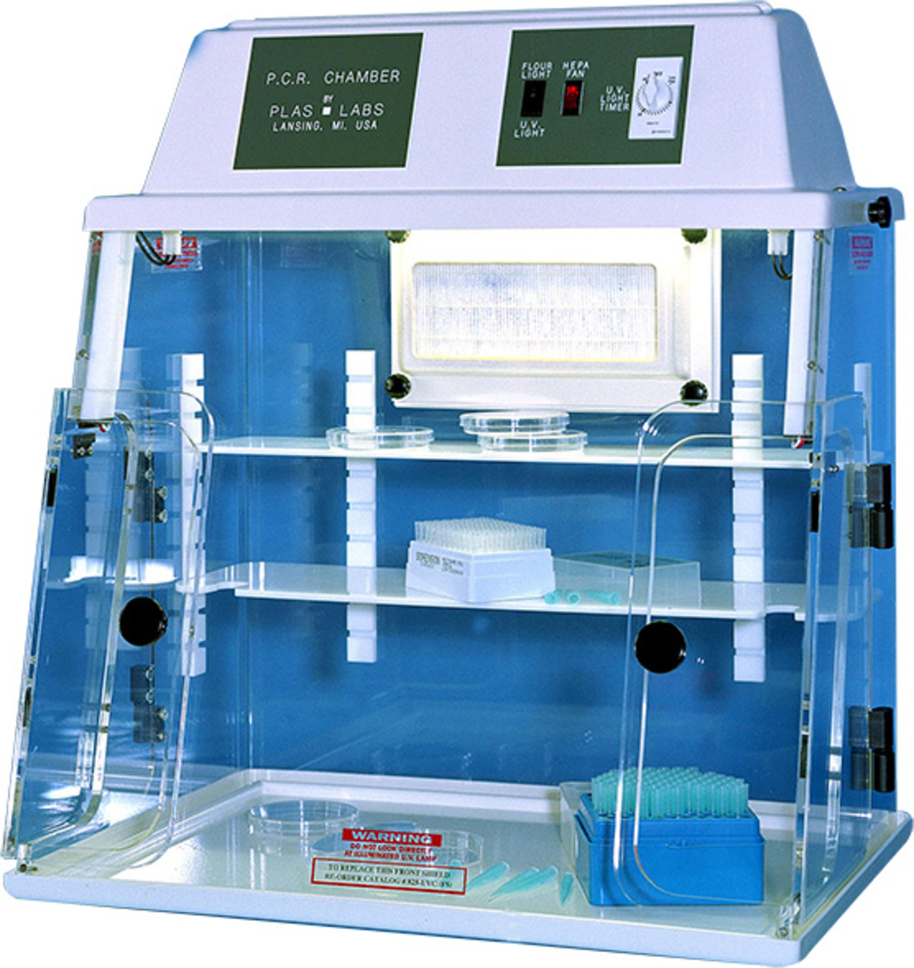
We manufacture cleanroom-grade Semiconductor Glove Boxes equipped with internal HEPA or ULPA filtration loops, delivering localized ISO Class 1 to Class 3 cleanliness levels. Our designs feature brushed or mirror-polished stainless steel structures to minimize particle shedding, active static-neutralizing ionizing bars to mitigate ESD risks, and custom flanges matching PVD/sputtering ports for seamless wafer transfers.